
A Practical Antenna Design and Integration Guide
As AIoT devices become more widespread, users expect more than basic wireless connectivity. They expect pairing to be fast, intuitive and nearly effortless.
Bluetooth remains one of the most widely used technologies for connecting smart hardware to smartphones and other devices. However, the conventional pairing process—opening settings, searching for the device, selecting the correct name and confirming the connection—can create unnecessary friction during product setup.
NFC-assisted Bluetooth pairing provides a more intuitive alternative. Bluetooth pairing information can be stored in an NFC tag or NFC-enabled device. When the user brings an NFC-compatible smartphone close to the product, the phone reads the pairing data and initiates the Bluetooth connection process.
Instead of asking users to search through a list of devices, NFC turns setup into a simple tap-and-confirm experience.
This article explains how NFC-assisted Bluetooth pairing works, why the NFC antenna is critical to the user experience, and how antenna placement, ferrite materials and connection methods affect performance in production-ready AI hardware.
From Manual Bluetooth Discovery to One-Tap Pairing
Many smart products still require instructions such as:
“Open your phone’s Bluetooth settings, search for the device and select it to pair.”
This process can be inconvenient for AI speakers, smart fitness mirrors, access terminals, industrial handheld devices and other connected products.
With NFC-assisted Bluetooth pairing, the device can operate as an NFC tag or NFC handover endpoint containing information such as:
- Bluetooth device address
- Device identification information
- Bluetooth Out-of-Band pairing data
- Supported carrier or connection information
- Other application-specific configuration data
When an NFC-enabled smartphone approaches the designated touch area, it reads the information and initiates the relevant pairing or connection workflow. Depending on the smartphone, operating system and implementation, the user may only need to confirm the connection.
The NFC Forum defines Connection Handover as a mechanism through which NFC devices can establish connections using other wireless technologies, including Bluetooth and Wi-Fi.
Traditional Bluetooth Pairing vs. NFC-Assisted Pairing
| Comparison | Traditional Bluetooth Pairing | NFC-Assisted Bluetooth Pairing |
|---|---|---|
| User interaction | Open settings, search, select and confirm | Tap or bring the phone close, then confirm |
| Setup time | Approximately 10–30 seconds | Potentially completed within a few seconds |
| Ease of use | Requires users to understand the device-discovery process | Provides a more physical and intuitive interaction |
| Device selection | Users may see several devices with similar names | The intended device can be identified directly |
| Setup experience | More steps and more opportunities for error | Faster and more controlled onboarding |
Actual pairing behavior and completion time depend on the smartphone operating system, Bluetooth implementation and application permissions.
Selecting the NFC and Bluetooth Architecture
The first architectural decision is whether to use an integrated wireless SoC or a separate NFC controller or tag IC.
A multiprotocol SoC, such as a suitable device in Nordic Semiconductor’s nRF52 family, can combine Bluetooth Low Energy functionality with an NFC-A tag peripheral. This approach can reduce component count and simplify compact product designs.
A separate NFC reader, controller or tag IC can provide greater flexibility when the system requires advanced NFC functions, higher output power, specialized reader modes or independent power management.
For example, STMicroelectronics introduced the ST25R200 NFC reader/writer IC for contactless applications requiring robust RF performance, noise management and low-power operation.
However, selecting an advanced IC does not guarantee a reliable tap experience. The NFC antenna remains the physical interface through which RF energy and data are exchanged.
Its design directly affects:
- Activation and read distance
- Touch-position tolerance
- Communication stability
- Smartphone compatibility
- Resistance to detuning
- Integration with the product enclosure
- Production consistency
A poorly integrated antenna may force users to move the phone repeatedly across the product or may fail to activate at all. Reliable one-tap pairing therefore requires the NFC IC, antenna, matching circuit, enclosure and nearby materials to be designed as one system.
The Main Design Challenge: NFC Antennas Near Metal
Compact AI hardware often contains batteries, displays, PCBs, shielding cans, metal brackets and decorative metal surfaces. These materials can significantly affect an NFC antenna.
At 13.56 MHz, the alternating magnetic field generated by the antenna can induce eddy currents in nearby metal. These currents create an opposing magnetic field that may:
- Reduce magnetic-field strength
- Shift the antenna’s resonant frequency
- Lower the quality factor
- Reduce read or activation distance
- Create inconsistent performance between installations
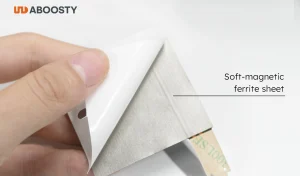
One common solution is to place a soft-magnetic ferrite sheet between the NFC antenna and the nearby metal surface.
The ferrite material provides a controlled, lower-reluctance path for magnetic flux, helping isolate the antenna from conductive components. When correctly selected and tuned, it can improve antenna efficiency and communication reliability near batteries, displays, PCB ground planes and metal enclosures.
Ferrite material should not be selected by thickness alone. Its permeability, magnetic loss, operating frequency, adhesive structure and mechanical placement must also be considered.
- ABOOSTY can support the complete integration process, including:
- Electromagnetic simulation
- Antenna geometry design
- Ferrite material selection
- Matching-circuit optimization
- Prototype testing
- In-device tuning
- Production verification
Designing the NFC Antenna for Efficient Manufacturing
Antenna performance is only one part of a successful product. The connection and assembly method also affects manufacturing cost, reliability and first-pass yield.
Manual soldering or crimping can increase assembly time and introduce operator-dependent variation. For suitable designs, an FPC connector provides a standardized connection method that can simplify assembly.
Depending on the available space and reliability requirements, possible connection methods include:
- Non-ZIF FPC connectors
- ZIF FPC connectors
- Micro-coaxial cable connections
- Wire-to-board crimp terminals
- PH-series wire connectors
- Direct soldering
The final connection method should be selected according to antenna structure, current RF design, installation distance, vibration level, production volume and serviceability requirements.
Recommended ABOOSTY NFC Antenna Options
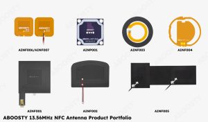
| NFC Antenna Model | Recommended Connector Type | Connector Model | Flexible PCB Thickness / Cable Requirements | Key Features and Typical Applications |
|---|---|---|---|---|
| AINF003 | Direct-insertion Flexible PCB connector (Non-ZIF) | Molex 512811000-SD receptacle, 0.5 mm pitch | Total thickness: approximately 0.3 mm; contact fingers reinforced to 0.2 mm and gold-plated | Ultra-thin and compact. Suitable for smartwatches, earbud charging cases and other devices with extremely limited internal space. Supports SMT assembly. |
| AINF003 | Direct-insertion Flexible PCB connector (ZIF) | Hirose FH12 series or equivalent | Total thickness: approximately 0.2 mm; standard contact fingers | Flip-lock design for a more reliable connection. Suitable for devices exposed to light vibration, such as handheld scanners. |
| IPEX micro-coaxial connection | First-generation IPEX connector (MHF I) | Soldered 1.13 mm-diameter coaxial cable; customizable cable length | Excellent high-frequency shielding and stable signal transmission. Suitable for larger smart devices where the antenna must be installed away from the main PCB. | |
| AINF007 | Crimped wire-terminal connection | Wire-side: Molex 51065-0200Board-side: Molex 502128000 | UL1007, 24–26 AWG wire | Most cost-effective option with a secure connection. Suitable for budget-sensitive devices with sufficient installation space and less demanding high-frequency performance requirements. |
| AINF002 | PH1.25 2-pin connector | Housing: PH-2PTerminal: SPH-002T-P0.5S, compatible with AWG28 | Thickness: 0.25 ± 0.1 mm; pre-installed UL1571 red-and-black twisted-pair cable with customizable length | Plug-and-play with high assembly efficiency. Suitable for smart cabinets, access-control and attendance terminals, industrial PDAs, shared equipment and other standardized products requiring fast integration. |
Connector compatibility and FPC thickness must be confirmed against the final antenna drawing and connector specification before production.
FPC Material and Soldering Reliability
Where cables or terminals must be soldered directly to an FPC antenna, copper type, pad structure and soldering temperature can affect long-term reliability.
Rolled-annealed copper and electrodeposited copper have different mechanical properties. Repeated bending, excessive soldering temperature or an unsuitable pad design may cause pad lifting or conductor damage.
For production projects, the following factors should be validated:
- FPC copper type and thickness
- Pad dimensions
- Stiffener design
- Soldering temperature and dwell time
- Cable strain relief
- Pull-force requirements
- Bending radius
- Assembly repeatability
These checks are particularly important when the antenna is installed in a product that experiences vibration, repeated handling or thermal cycling.
Recommendations From an Antenna Engineer With Over 20 Years of Experience
ABOOSTY has supported NFC integration in smart speakers, smart-home control panels, facial-recognition terminals and other connected devices.
There is no universal NFC antenna that performs identically in every product. Antenna performance must be evaluated in the final mechanical environment because every application has different:
- Available dimensions
- Enclosure materials
- Metal structures
- Battery and display locations
- PCB ground-plane geometry
- Smartphone approach direction
- Assembly conditions
ABOOSTY offers two development paths.
1. Select a Standard NFC Antenna
For projects with conventional mechanical requirements, engineers can compare existing ABOOSTY NFC antenna models according to antenna shape, size, installation method and application.
This approach can shorten the evaluation cycle and reduce initial development cost.
2. Develop a Custom NFC Antenna
When a standard antenna cannot meet the required dimensions, touch position, read distance or metal-environment performance, ABOOSTY can provide a customized solution covering:
- Requirements analysis
- Antenna design
- Electromagnetic simulation
- Matching-circuit design
- Prototype production
- In-device RF testing
- Performance optimization
- Mass production
The antenna should be considered during the early mechanical-design stage. Early integration can prevent costly enclosure changes, PCB revisions and performance problems later in development.
Build a More Reliable One-Tap Pairing Experience
NFC-assisted Bluetooth pairing can significantly improve product onboarding, but the user experience depends on more than storing a Bluetooth address in an NFC tag.
A reliable solution requires coordinated design of the NFC antenna, ferrite layer, matching circuit, IC, enclosure, metal environment and assembly process.
If you are developing an AI speaker, smart display, access-control terminal, wearable device, industrial handheld or other connected product, send us:
- Device dimensions
- Available antenna space
- Enclosure material
- Nearby battery, display, PCB or metal components
- Required touch position
- Target activation distance
- Estimated production volume
Contact the ABOOSTY antenna engineering team for an initial NFC antenna assessment or a customized 13.56 MHz antenna solution.